
Small Chips Mean Big
|
 |
| The moment construction was completed in 2013, company officials announced multibillion dollar plans to expand the plant and begin construction on a research building nearby. |
Malta is where the world’s largest semiconductor manufacturer, GlobalFoundries, has been building their North American manufacturing campus. Since ground breaking July 2009, more than 3 million square feet of office, research and production facilities have been built and total capital investment by the company is nearly $8 billion. Production began less than 18 months later, and company officials have already announced plans for an additional $9-10 billion to expand the facility.
The GlobalFoundries project is also the largest private project labor agreement in IBEW history, according to the IBEW’s business development office.
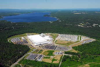 |
| The GlobalFoundries’ Malta, N.Y. semiconductor fabrication plant, is among the largest private construction projects in the country, and the IBEW’s largest project labor agreement. |
“We have averaged two-million plus man-hours every year since 2009. No less than 200 members have been on site since groundbreaking and we’ve had up to 800,” said Albany, N.Y., Local 236 Business Manager Don Rahm. “If I had to guess, I think it will be another 10 to 15 years before things level out and they stop expanding. The future looks very bright.”
Third District International Vice President Donald C. Siegel said the project is notable not just for its size but for how smoothly the work has gone.
“Generally, when a project is this big, you expect to have problems and we haven’t heard anything like that, and that is a very good thing,” Siegel said. “That tells me this is a well-designed PLA and it says a lot about the workmanship and integrity of our people in Local 236 and the influence of the code of excellence on us all.”
Company officials also said that construction has been notably free of drama.
“The campus has successfully hit all major construction, operations and customer milestones, and is fulfilling its mission to ramp on existing manufacturing production technology while in parallel developing advanced manufacturing technologies on future production nodes,” said a company spokesman.
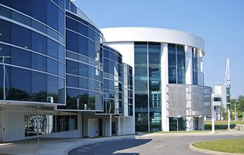 |
| The College of Nanoscale Science and Engineering at the State University of New York at Albany has become a research hub for global chip makers industry and a boon for the IBEW members who have been building it over the last decade. |
Rahm says he and members of the building trades have been in conversation with GlobalFoundries about extending the PLA should the company build a second chip fabrication plant at the site. Siegel and Rahm are confident that the members of Local 236 have proven their value over the last five years.
“Why would they change the formula when it has been working so well?” Siegel said.
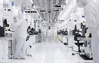
There are only so many different ways to build a building, but Rahm says there is a very steep learning curve working in the heart of the plant, the 300,000-square-foot clean room where the chips are made. As big as six football fields, it must be kept entirely free of dust and contaminants. Workers have to wear special clean suits and masks, wash all parts, including conduit inside and out, and follow detailed instructions for installations.
“The protocols are specific –extremely specific—and while doing the work precisely is not specialized, doing it efficiently and precisely is,” Rahm said.
Before Fab 8’s construction, semiconductor production was shrinking in the U.S. Nearly all chip engineering and design happens in the U.S., but for several decades, new factories were built in Europe and Asia, not in the U.S.
Nearly a decade ago, New York launched an aggressive campaign to turn that around. Aggressive subsidies were announced –GlobalFoundries has received significant tax incentives and grants over the last decade-- and a former rocket and missile fuels testing ground was cleaned up and converted into the Luther Forest Technology Campus, 1,400 acres pre-approved for semiconductor and nanotechnology manufacturing.
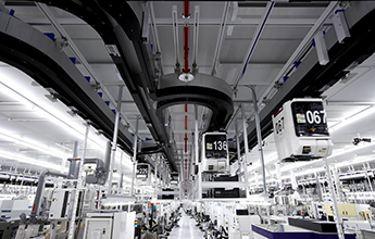 |
| Semiconductors are fabricated in the 300,000 square-foot clean room which is kept free of dust, chemicals and fumes. |
“The IBEW and the state building trades have been important partners at every step of this project,” Rahm said. “For years our members were at every planning, zoning and community meeting because we knew what it would mean for our members.”
In 2001, the state also established the College of Nanoscale Science and Engineering at the State University of New York at Albany. Over the last 13 years, more than $10 billion of public and private money has been spent on buildings and equipment at the site, another boon to Local 236.
“To be honest, the recession passed us by,” Rahm said.
Construction at CSNE is also expected to continue at a breakneck pace with ground-breakings planned in 2015 for a zero-net energy nanotech building and a science, technology and engineering high school.
“The enormity of it, I can barely get my head around these projects in the billions,” Rahm said. “We have been very fortunate.”
![]()